Search This Blog

Wednesday, March 9, 2011

Program to multiply two 8-bit data......

Program to Multiply two 8-bit data stored at memory location 2101H and 2102H.

For multiplication we will take one number as a reference keep it decrementing by one and the other number incrementing by magnitude equal to its value.

----------
LDA 2101H
MOVE B, A;
LDA 2102H;
MOVE C, A;
MVI D, 00H;
<A2> ADD C;
JC A1;
DCR B;
JZ EXITA4;
JMP A2;
<A1> INR D;
JMP A2
<EXITA4>HLT;
-------------------

Program to find teo's Complement......

Program to find two's complement of data stored at memory address 2100H....

For two's complement again we will use XRI operation and add 01H to its answers. Meaning we are finding ones complement then adding it with 1 to get the twos complement.

----------
LDA 2100H;
XRI FFH;
ADI A, 01;
STA 2101H;
HLT;
-----------

Program to find one's Complement....

Program to find one's complement of data stored at memory address 2100H....

For finding one's complement we will use XRI operation......

-------------
LDA 2100H;
XRI FF;
STA 2101H;
HLT;
-------------

Program that takes two nibbles......

Program that takes two nibbles from 2100H and 2101H and combines to form a byte. The nibbles from 2100 are to be taken as most significant nibble.

To extract a nibble we will use the Anding operation....
-----------
LDA 2100H;
ANI F0;
MOVE B,A;
LDA 2101H;
ANI 0F;
ADD B;
STA 2103H;
HLT;
-----------

Chapter Links to Understand Assembly language

Chapter - 1 : The Concepts
Chapter - 2 : Inside the ARM
Chapter - 3 : The Instruction Set
Chapter - 4 : Basic Assembler
Chapter - 6 : Data Structures
Chapter - 7 : Non User Modes

Appendix - 3 : Instruction Set

----------

Pdf Links
00toc.pdf               31-Oct-2005 10:31    21k  
[   ] 01ch.pdf                31-Oct-2005 10:31   139k  
[   ] 02ach.pdf               31-Oct-2005 10:31   152k  
[   ] 02ch.pdf                31-Oct-2005 10:31   123k  
[   ] 03ch.pdf                31-Oct-2005 10:31   180k  
[   ] 04ch.pdf                31-Oct-2005 10:31   144k  
[   ] 05ach.pdf               31-Oct-2005 10:31   291k  
[   ] 05ch.pdf                31-Oct-2005 10:31   156k  
[   ] 06ach.pdf               31-Oct-2005 10:31   382k  
[   ] 06ch.pdf                31-Oct-2005 10:32   184k  
[   ] 07ach.pdf               31-Oct-2005 10:32   216k  
[   ] 07ch.pdf                31-Oct-2005 10:32   118k  
[   ] 08app1.pdf              31-Oct-2005 10:32   112k  
[   ] 09app2.pdf              31-Oct-2005 10:32   123k  
[   ] 10app3.pdf              31-Oct-2005 10:33    29k  
[   ] 11index.pdf             31-Oct-2005 10:33    61k  
[TXT] ReadMe.txt              31-Oct-2005 10:34     1k 
--------------- 

Sample Programs

Program to multiply a number by 8
---------------
MVI A, 30H
RRC
RRC
RRC
OUT PORT1
HLT
----------------

Program to find greatest between two numbers
----------------
MVI B, 30H
MVI C, 40H
MOV A, B
CMP C
JZ EQU
JC GRT
OUT PORT1
HLT
EQU: MVI A, 01H
OUT PORT1
HLT
GRT: MOV A, C
OUT PORT1
HLT
----------------

Instruction Set Classification

An instruction is a binary pattern designed inside a microprocessor to perform a specific function. The entire group of instructions, called the instruction set, determines what functions the microprocessor can perform. These instructions can be classified into the following five functional categories: data transfer (copy) operations, arithmetic operations, logical operations, branching operations, and machine-control operations.

Data Transfer (Copy) Operations
This group of instructions copy data from a location called a source to another location called a destination, without modifying the contents of the source. In technical manuals, the term data transfer is used for this copying function. However, the term transfer is misleading; it creates the impression that the contents of the
source are destroyed when, in fact, the contents are retained without any modification. The various types of data transfer (copy) are listed below together with examples of each type:

Table 1
Arithmetic Operations
These instructions perform arithmetic operations such as addition, subtraction, increment, and decrement.
Addition - Any 8-bit number, or the contents of a register or the contents of a memory location can be added to the contents of the accumulator and the sum is stored in the accumulator. No two other 8-bit registers can be added directly (e.g., the contents of register B cannot be added directly to the contents of the register C). The instruction DAD is an exception; it adds 16-bit data directly in register pairs.

Subtraction - Any 8-bit number, or the contents of a register, or the contents of a memory location can be subtracted from the contents of the accumulator and the results stored in the accumulator. The subtraction is performed in 2's compliment, and the results if negative, are expressed in 2's complement. No two other registers can be subtracted directly.

Increment/Decrement - The 8-bit contents of a register or a memory location can be incremented or decrement by 1. Similarly, the 16-bit contents of a register pair (such as BC) can be incremented or decrement by 1. These increment and decrement operations differ from addition and subtraction in an important way; i.e., they can be performed in any one of the registers or in a memory location.

Logical Operations
These instructions perform various logical operations with the contents of the accumulator.
AND, OR Exclusive-OR - Any 8-bit number, or the contents of a register, or of a memory location can be logically ANDed, Ored, or Exclusive-ORed with the contents of the accumulator. The results are stored in the accumulator.

Rotate- Each bit in the accumulator can be shifted either left or right to the next position.

Compare- Any 8-bit number, or the contents of a register, or a memory location can be compared for equality, greater than, or less than, with the contents of the accumulator.

Complement - The contents of the accumulator can be complemented. All 0s are replaced by 1s and all 1s are replaced by 0s.

Branching Operations
This group of instructions alters the sequence of program execution either conditionally or unconditionally.

Jump - Conditional jumps are an important aspect of the decision-making process in the programming. These instructions test for a certain conditions (e.g., Zero or Carry flag) and alter the program sequence when the condition is met. In addition, the instruction set includes an instruction called unconditional jump.

Call, Return, and Restart - These instructions change the sequence of a program either by calling a subroutine or returning from a subroutine. The conditional Call and Return instructions also can test condition flags.

Machine Control Operations
These instructions control machine functions such as Halt, Interrupt, or do nothing. The microprocessor operations related to data manipulation can be summarized in four functions:
  • 1. copying data
  • 2. performing arithmetic operations
  • 3. performing logical operations
  • 4. testing for a given condition and alerting the program sequence
Some important aspects of the instruction set are noted below:
  • 1. In data transfer, the contents of the source are not destroyed; only the contents of the destination are changed. The data copy instructions do not affect the flags.
  • 2. Arithmetic and Logical operations are performed with the contents of the accumulator, and the results are stored in the accumulator (with some expectations). The flags are affected according to the results.
  • 3. Any register including the memory can be used for increment and decrement.
  • 4. A program sequence can be changed either conditionally or by testing for a given data condition.
------------

The 8085 Addressing Modes

The instructions MOV B, A or MVI A, 82H are to copy data from a source into a destination. In these instructions the source can be a register, an input port, or an 8-bit number (00H to FFH). Similarly, a destination can be a register or an output port. The sources and destination are operands. The various formats for specifying operands are called the ADDRESSING MODES. For 8085, they are:
1. Immediate addressing.
2. Register addressing.
3. Direct addressing.
4. Indirect addressing.
Immediate addressing
Data is present in the instruction. Load the immediate data to the destination provided.
Example: MVI R,data
Register addressing
Data is provided through the registers.
Example: MOV Rd, Rs
Direct addressing
Used to accept data from outside devices to store in the accumulator or send the data stored in the accumulator to the outside device. Accept the data from the port 00H and store them into the accumulator or Send the data from the accumulator to the port 01H.
Example: IN 00H or OUT 01H
Indirect Addressing
This means that the Effective Address is calculated by the processor. And the contents of the address (and the one following) is used to form a second address. The second address is where the data is stored. Note that this requires several memory accesses; two accesses to retrieve the 16-bit address and a further access (or accesses) to retrieve the data which is to be loaded into the register.
-----------

The 8085 Programming Model

The 8085 programming model includes six registers, one accumulator, and one flag register, Figure. In  addition, it has two 16-bit registers: the stack pointer and the program counter. They are described briefly as follows.
Register Diagram

Registers
The 8085 has six general-purpose registers to store 8-bit data; these are identified as B,C,D,E,H, and L as shown in the figure. They can be combined as register pairs - BC, DE, and HL - to perform some 16-bit operations. The programmer can use these registers to store or copy data into the registers by using data copy instructions.

Accumulator
The accumulator is an 8-bit register that is a part of arithmetic/logic unit (ALU). This register is used to store 8-bit data and to perform arithmetic and logical operations. The result of an operation is stored in the accumulator. The accumulator is also identified as register A.
ACCUMULATOR A (8) FLAG REGISTER
B (8)
D (8)
H (8)
Stack Pointer (SP) (16)
Program Counter (PC) (16)
C (8)
E (8)
L (8)
Data Bus Address Bus
8 Lines Bidirectional 16 Lines unidirectional
 
Flags
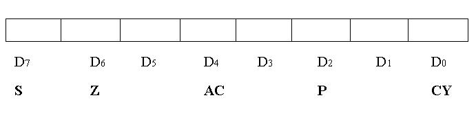
The ALU includes five flip-flops, which are set or reset after an operation according to data conditions of the result in the accumulator and other registers. They are called Zero(Z), Carry (CY), Sign (S), Parity (P), and Auxiliary Carry (AC) flags; their bit positions in the flag register are shown in the Figure below. The most commonly used flags are Zero, Carry, and Sign. The microprocessor uses these flags to test data conditions.
Flags

For example, after an addition of two numbers, if the sum in the accumulator id larger than eight bits, the flip-flop uses to indicate a carry -- called the Carry flag (CY) -- is set to one. When an arithmetic operation results in zero, the flip-flop called the Zero(Z) flag is set to one. The first Figure shows an 8-bit register, called the flag register, adjacent to the accumulator. However, it is not used as a register; five bit positions out of eight are used to store the outputs of the five flip-flops. The flags are stored in the 8-bit register so that the programmer can examine these flags (data conditions) by accessing the register through an instruction.
These flags have critical importance in the decision-making process of the microprocessor. The conditions (set or reset) of the flags are tested through the software instructions. For example, the instruction JC (Jump on Carry) is implemented to change the sequence of a program when CY flag is set. The thorough understanding of flag is essential in writing assembly language programs.
 
Program Counter (PC)
This 16-bit register deals with sequencing the execution of instructions. This register is a memory pointer. Memory locations have 16-bit addresses, and that is why this is a 16-bit register.
The microprocessor uses this register to sequence the execution of the instructions. The function of the program counter is to point to the memory address from which the next byte is to be fetched. When a byte (machine code) is being fetched, the program counter is incremented by one to point to the next memory location
 
Stack Pointer (SP)
The stack pointer is also a 16-bit register used as a memory pointer. It points to a memory location in R/W memory, called the stack. The beginning of the stack is defined by loading 16-bit address in the stack pointer.
This programming model will be used in subsequent tutorials to examine how these registers are affected after the execution of an instruction.
--------------

Tuesday, March 8, 2011

8085 Functional Description

Functional Diagram
The 8085A is a complete 8 bit parallel central processor. It requires a single +5 volt supply. Its basic clock speed is 3 MHz thus improving on the present 8080's performance with higher system speed. Also it is designed to fit into a minimum system of three IC's: The CPU, a RAM/ IO, and a ROM or PROM/IO chip.
The 8085A uses a multiplexed Data Bus. The address is split between the higher 8bit Address Bus and the lower 8bit Address/Data Bus. During the first cycle the address is sent out. The lower 8bits are latched into the peripherals by the Address Latch Enable (ALE). During the rest of the machine cycle the Data Bus is used for memory or l/O data.

The 8085A provides RD, WR, and lO/Memory signals for bus control. An Interrupt Acknowledge signal (INTA) is also provided. Hold, Ready, and all Interrupts are synchronized. The 8085A also provides serial input data (SID) and serial output data (SOD) lines for simple serial interface. In addition to these features, the 8085A has three maskable, restart interrupts and one non-maskable trap interrupt. The 8085A provides RD, WR and IO/M signals for Bus control.
Status Information
Status information is directly available from the 8085A. ALE serves as a status strobe. The status is partially encoded, and provides the user with advanced timing of the type of bus transfer being done. IO/M cycle status signal is provided directly also. Decoded So, S1 Carries the following status information:
HALT, WRITE, READ, FETCH S1 can be interpreted as R/W in all bus transfers. In the 8085A the 8 LSB of address are multiplexed with the data instead of status. The ALE line is used as a strobe to enter the lower half of the address into the memory or peripheral address latch. This also frees extra pins for expanded interrupt capability.

Interrupt and Serial l/O
The8085A has5 interrupt inputs: INTR, RST5.5, RST6.5, RST 7.5, and TRAP. INTR is identical in function to the 8080 INT. Each of the three RESTART inputs, 5.5, 6.5. 7.5, has a programmable mask. TRAP is also a RESTART interrupt except it is nonmaskable. The three RESTART interrupts cause the internal execution of RST (saving the program counter in the stack and branching to the RESTART address) if the interrupts are enabled and if the interrupt mask is not set. The non-maskable TRAP causes the internal execution of a RST independent of the state of the interrupt enable or masks. The interrupts are arranged in a fixed priority that determines which interrupt is to be recognized if more than one is pending as follows: TRAP highest priority, RST 7.5, RST 6.5, RST 5.5, INTR lowest priority This priority scheme does not take into account the priority of a routine that was started by a higher priority interrupt. RST 5.5 can interrupt a RST 7.5 routine if the interrupts were re-enabled before the end of the RST 7.5 routine. The TRAP interrupt is useful for catastrophic errors such as power failure or bus error. The TRAP input is recognized just as any other interrupt but has the highest priority. It is not affected by any flag or mask. The TRAP input is both edge and level sensitive.

Basic System Timing
The 8085A has a multiplexed Data Bus. ALE is used as a strobe to sample the lower 8bits of address on the Data Bus. Figure 2 shows an instruction fetch, memory read and l/ O write cycle (OUT). Note that during the l/O write and read cycle that the l/O port address is copied on both the upper and lower half of the address. As in the 8080, the READY line is used to extend the read and write pulse lengths so that the 8085A can be used with slow memory. Hold causes the CPU to relingkuish the bus when it is through with it by floating the Address and Data Buses.

System Interface
8085A family includes memory components, which are directly compatible to the 8085A CPU. For example, a system consisting of the three chips, 8085A, 8156, and 8355 will have the following features:
· 2K Bytes ROM
· 256 Bytes RAM
· 1 Timer/Counter
· 4 8bit l/O Ports
· 1 6bit l/O Port
· 4 Interrupt Levels
· Serial In/Serial Out Ports
In addition to standard l/O, the memory mapped I/O offers an efficient l/O addressing technique. With this technique, an area of memory address space is assigned for l/O address, thereby, using the memory address for I/O manipulation. The 8085A CPU can also interface with the standard memory that does not have the multiplexed address/data bus.
--------------