Search This Blog

Wednesday, March 9, 2011

Program to multiply two 8-bit data......

Program to Multiply two 8-bit data stored at memory location 2101H and 2102H.

For multiplication we will take one number as a reference keep it decrementing by one and the other number incrementing by magnitude equal to its value.

----------
LDA 2101H
MOVE B, A;
LDA 2102H;
MOVE C, A;
MVI D, 00H;
<A2> ADD C;
JC A1;
DCR B;
JZ EXITA4;
JMP A2;
<A1> INR D;
JMP A2
<EXITA4>HLT;
-------------------

Program to find teo's Complement......

Program to find two's complement of data stored at memory address 2100H....

For two's complement again we will use XRI operation and add 01H to its answers. Meaning we are finding ones complement then adding it with 1 to get the twos complement.

----------
LDA 2100H;
XRI FFH;
ADI A, 01;
STA 2101H;
HLT;
-----------

Program to find one's Complement....

Program to find one's complement of data stored at memory address 2100H....

For finding one's complement we will use XRI operation......

-------------
LDA 2100H;
XRI FF;
STA 2101H;
HLT;
-------------

Program that takes two nibbles......

Program that takes two nibbles from 2100H and 2101H and combines to form a byte. The nibbles from 2100 are to be taken as most significant nibble.

To extract a nibble we will use the Anding operation....
-----------
LDA 2100H;
ANI F0;
MOVE B,A;
LDA 2101H;
ANI 0F;
ADD B;
STA 2103H;
HLT;
-----------

Chapter Links to Understand Assembly language

Chapter - 1 : The Concepts
Chapter - 2 : Inside the ARM
Chapter - 3 : The Instruction Set
Chapter - 4 : Basic Assembler
Chapter - 6 : Data Structures
Chapter - 7 : Non User Modes

Appendix - 3 : Instruction Set

----------

Pdf Links
00toc.pdf               31-Oct-2005 10:31    21k  
[   ] 01ch.pdf                31-Oct-2005 10:31   139k  
[   ] 02ach.pdf               31-Oct-2005 10:31   152k  
[   ] 02ch.pdf                31-Oct-2005 10:31   123k  
[   ] 03ch.pdf                31-Oct-2005 10:31   180k  
[   ] 04ch.pdf                31-Oct-2005 10:31   144k  
[   ] 05ach.pdf               31-Oct-2005 10:31   291k  
[   ] 05ch.pdf                31-Oct-2005 10:31   156k  
[   ] 06ach.pdf               31-Oct-2005 10:31   382k  
[   ] 06ch.pdf                31-Oct-2005 10:32   184k  
[   ] 07ach.pdf               31-Oct-2005 10:32   216k  
[   ] 07ch.pdf                31-Oct-2005 10:32   118k  
[   ] 08app1.pdf              31-Oct-2005 10:32   112k  
[   ] 09app2.pdf              31-Oct-2005 10:32   123k  
[   ] 10app3.pdf              31-Oct-2005 10:33    29k  
[   ] 11index.pdf             31-Oct-2005 10:33    61k  
[TXT] ReadMe.txt              31-Oct-2005 10:34     1k 
--------------- 

Sample Programs

Program to multiply a number by 8
---------------
MVI A, 30H
RRC
RRC
RRC
OUT PORT1
HLT
----------------

Program to find greatest between two numbers
----------------
MVI B, 30H
MVI C, 40H
MOV A, B
CMP C
JZ EQU
JC GRT
OUT PORT1
HLT
EQU: MVI A, 01H
OUT PORT1
HLT
GRT: MOV A, C
OUT PORT1
HLT
----------------

Instruction Set Classification

An instruction is a binary pattern designed inside a microprocessor to perform a specific function. The entire group of instructions, called the instruction set, determines what functions the microprocessor can perform. These instructions can be classified into the following five functional categories: data transfer (copy) operations, arithmetic operations, logical operations, branching operations, and machine-control operations.

Data Transfer (Copy) Operations
This group of instructions copy data from a location called a source to another location called a destination, without modifying the contents of the source. In technical manuals, the term data transfer is used for this copying function. However, the term transfer is misleading; it creates the impression that the contents of the
source are destroyed when, in fact, the contents are retained without any modification. The various types of data transfer (copy) are listed below together with examples of each type:

Table 1
Arithmetic Operations
These instructions perform arithmetic operations such as addition, subtraction, increment, and decrement.
Addition - Any 8-bit number, or the contents of a register or the contents of a memory location can be added to the contents of the accumulator and the sum is stored in the accumulator. No two other 8-bit registers can be added directly (e.g., the contents of register B cannot be added directly to the contents of the register C). The instruction DAD is an exception; it adds 16-bit data directly in register pairs.

Subtraction - Any 8-bit number, or the contents of a register, or the contents of a memory location can be subtracted from the contents of the accumulator and the results stored in the accumulator. The subtraction is performed in 2's compliment, and the results if negative, are expressed in 2's complement. No two other registers can be subtracted directly.

Increment/Decrement - The 8-bit contents of a register or a memory location can be incremented or decrement by 1. Similarly, the 16-bit contents of a register pair (such as BC) can be incremented or decrement by 1. These increment and decrement operations differ from addition and subtraction in an important way; i.e., they can be performed in any one of the registers or in a memory location.

Logical Operations
These instructions perform various logical operations with the contents of the accumulator.
AND, OR Exclusive-OR - Any 8-bit number, or the contents of a register, or of a memory location can be logically ANDed, Ored, or Exclusive-ORed with the contents of the accumulator. The results are stored in the accumulator.

Rotate- Each bit in the accumulator can be shifted either left or right to the next position.

Compare- Any 8-bit number, or the contents of a register, or a memory location can be compared for equality, greater than, or less than, with the contents of the accumulator.

Complement - The contents of the accumulator can be complemented. All 0s are replaced by 1s and all 1s are replaced by 0s.

Branching Operations
This group of instructions alters the sequence of program execution either conditionally or unconditionally.

Jump - Conditional jumps are an important aspect of the decision-making process in the programming. These instructions test for a certain conditions (e.g., Zero or Carry flag) and alter the program sequence when the condition is met. In addition, the instruction set includes an instruction called unconditional jump.

Call, Return, and Restart - These instructions change the sequence of a program either by calling a subroutine or returning from a subroutine. The conditional Call and Return instructions also can test condition flags.

Machine Control Operations
These instructions control machine functions such as Halt, Interrupt, or do nothing. The microprocessor operations related to data manipulation can be summarized in four functions:
  • 1. copying data
  • 2. performing arithmetic operations
  • 3. performing logical operations
  • 4. testing for a given condition and alerting the program sequence
Some important aspects of the instruction set are noted below:
  • 1. In data transfer, the contents of the source are not destroyed; only the contents of the destination are changed. The data copy instructions do not affect the flags.
  • 2. Arithmetic and Logical operations are performed with the contents of the accumulator, and the results are stored in the accumulator (with some expectations). The flags are affected according to the results.
  • 3. Any register including the memory can be used for increment and decrement.
  • 4. A program sequence can be changed either conditionally or by testing for a given data condition.
------------

The 8085 Addressing Modes

The instructions MOV B, A or MVI A, 82H are to copy data from a source into a destination. In these instructions the source can be a register, an input port, or an 8-bit number (00H to FFH). Similarly, a destination can be a register or an output port. The sources and destination are operands. The various formats for specifying operands are called the ADDRESSING MODES. For 8085, they are:
1. Immediate addressing.
2. Register addressing.
3. Direct addressing.
4. Indirect addressing.
Immediate addressing
Data is present in the instruction. Load the immediate data to the destination provided.
Example: MVI R,data
Register addressing
Data is provided through the registers.
Example: MOV Rd, Rs
Direct addressing
Used to accept data from outside devices to store in the accumulator or send the data stored in the accumulator to the outside device. Accept the data from the port 00H and store them into the accumulator or Send the data from the accumulator to the port 01H.
Example: IN 00H or OUT 01H
Indirect Addressing
This means that the Effective Address is calculated by the processor. And the contents of the address (and the one following) is used to form a second address. The second address is where the data is stored. Note that this requires several memory accesses; two accesses to retrieve the 16-bit address and a further access (or accesses) to retrieve the data which is to be loaded into the register.
-----------

The 8085 Programming Model

The 8085 programming model includes six registers, one accumulator, and one flag register, Figure. In  addition, it has two 16-bit registers: the stack pointer and the program counter. They are described briefly as follows.
Register Diagram

Registers
The 8085 has six general-purpose registers to store 8-bit data; these are identified as B,C,D,E,H, and L as shown in the figure. They can be combined as register pairs - BC, DE, and HL - to perform some 16-bit operations. The programmer can use these registers to store or copy data into the registers by using data copy instructions.

Accumulator
The accumulator is an 8-bit register that is a part of arithmetic/logic unit (ALU). This register is used to store 8-bit data and to perform arithmetic and logical operations. The result of an operation is stored in the accumulator. The accumulator is also identified as register A.
ACCUMULATOR A (8) FLAG REGISTER
B (8)
D (8)
H (8)
Stack Pointer (SP) (16)
Program Counter (PC) (16)
C (8)
E (8)
L (8)
Data Bus Address Bus
8 Lines Bidirectional 16 Lines unidirectional
 
Flags
The ALU includes five flip-flops, which are set or reset after an operation according to data conditions of the result in the accumulator and other registers. They are called Zero(Z), Carry (CY), Sign (S), Parity (P), and Auxiliary Carry (AC) flags; their bit positions in the flag register are shown in the Figure below. The most commonly used flags are Zero, Carry, and Sign. The microprocessor uses these flags to test data conditions.
Flags

For example, after an addition of two numbers, if the sum in the accumulator id larger than eight bits, the flip-flop uses to indicate a carry -- called the Carry flag (CY) -- is set to one. When an arithmetic operation results in zero, the flip-flop called the Zero(Z) flag is set to one. The first Figure shows an 8-bit register, called the flag register, adjacent to the accumulator. However, it is not used as a register; five bit positions out of eight are used to store the outputs of the five flip-flops. The flags are stored in the 8-bit register so that the programmer can examine these flags (data conditions) by accessing the register through an instruction.
These flags have critical importance in the decision-making process of the microprocessor. The conditions (set or reset) of the flags are tested through the software instructions. For example, the instruction JC (Jump on Carry) is implemented to change the sequence of a program when CY flag is set. The thorough understanding of flag is essential in writing assembly language programs.
 
Program Counter (PC)
This 16-bit register deals with sequencing the execution of instructions. This register is a memory pointer. Memory locations have 16-bit addresses, and that is why this is a 16-bit register.
The microprocessor uses this register to sequence the execution of the instructions. The function of the program counter is to point to the memory address from which the next byte is to be fetched. When a byte (machine code) is being fetched, the program counter is incremented by one to point to the next memory location
 
Stack Pointer (SP)
The stack pointer is also a 16-bit register used as a memory pointer. It points to a memory location in R/W memory, called the stack. The beginning of the stack is defined by loading 16-bit address in the stack pointer.
This programming model will be used in subsequent tutorials to examine how these registers are affected after the execution of an instruction.
--------------

Tuesday, March 8, 2011

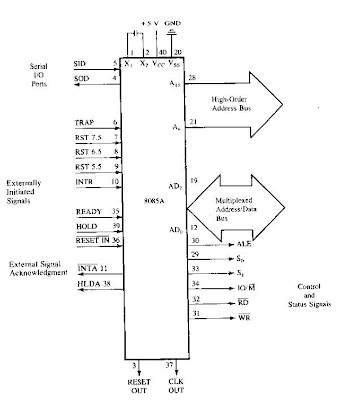
8085 Functional Description

Functional Diagram
The 8085A is a complete 8 bit parallel central processor. It requires a single +5 volt supply. Its basic clock speed is 3 MHz thus improving on the present 8080's performance with higher system speed. Also it is designed to fit into a minimum system of three IC's: The CPU, a RAM/ IO, and a ROM or PROM/IO chip.
The 8085A uses a multiplexed Data Bus. The address is split between the higher 8bit Address Bus and the lower 8bit Address/Data Bus. During the first cycle the address is sent out. The lower 8bits are latched into the peripherals by the Address Latch Enable (ALE). During the rest of the machine cycle the Data Bus is used for memory or l/O data.

The 8085A provides RD, WR, and lO/Memory signals for bus control. An Interrupt Acknowledge signal (INTA) is also provided. Hold, Ready, and all Interrupts are synchronized. The 8085A also provides serial input data (SID) and serial output data (SOD) lines for simple serial interface. In addition to these features, the 8085A has three maskable, restart interrupts and one non-maskable trap interrupt. The 8085A provides RD, WR and IO/M signals for Bus control.
Status Information
Status information is directly available from the 8085A. ALE serves as a status strobe. The status is partially encoded, and provides the user with advanced timing of the type of bus transfer being done. IO/M cycle status signal is provided directly also. Decoded So, S1 Carries the following status information:
HALT, WRITE, READ, FETCH S1 can be interpreted as R/W in all bus transfers. In the 8085A the 8 LSB of address are multiplexed with the data instead of status. The ALE line is used as a strobe to enter the lower half of the address into the memory or peripheral address latch. This also frees extra pins for expanded interrupt capability.

Interrupt and Serial l/O
The8085A has5 interrupt inputs: INTR, RST5.5, RST6.5, RST 7.5, and TRAP. INTR is identical in function to the 8080 INT. Each of the three RESTART inputs, 5.5, 6.5. 7.5, has a programmable mask. TRAP is also a RESTART interrupt except it is nonmaskable. The three RESTART interrupts cause the internal execution of RST (saving the program counter in the stack and branching to the RESTART address) if the interrupts are enabled and if the interrupt mask is not set. The non-maskable TRAP causes the internal execution of a RST independent of the state of the interrupt enable or masks. The interrupts are arranged in a fixed priority that determines which interrupt is to be recognized if more than one is pending as follows: TRAP highest priority, RST 7.5, RST 6.5, RST 5.5, INTR lowest priority This priority scheme does not take into account the priority of a routine that was started by a higher priority interrupt. RST 5.5 can interrupt a RST 7.5 routine if the interrupts were re-enabled before the end of the RST 7.5 routine. The TRAP interrupt is useful for catastrophic errors such as power failure or bus error. The TRAP input is recognized just as any other interrupt but has the highest priority. It is not affected by any flag or mask. The TRAP input is both edge and level sensitive.

Basic System Timing
The 8085A has a multiplexed Data Bus. ALE is used as a strobe to sample the lower 8bits of address on the Data Bus. Figure 2 shows an instruction fetch, memory read and l/ O write cycle (OUT). Note that during the l/O write and read cycle that the l/O port address is copied on both the upper and lower half of the address. As in the 8080, the READY line is used to extend the read and write pulse lengths so that the 8085A can be used with slow memory. Hold causes the CPU to relingkuish the bus when it is through with it by floating the Address and Data Buses.

System Interface
8085A family includes memory components, which are directly compatible to the 8085A CPU. For example, a system consisting of the three chips, 8085A, 8156, and 8355 will have the following features:
· 2K Bytes ROM
· 256 Bytes RAM
· 1 Timer/Counter
· 4 8bit l/O Ports
· 1 6bit l/O Port
· 4 Interrupt Levels
· Serial In/Serial Out Ports
In addition to standard l/O, the memory mapped I/O offers an efficient l/O addressing technique. With this technique, an area of memory address space is assigned for l/O address, thereby, using the memory address for I/O manipulation. The 8085A CPU can also interface with the standard memory that does not have the multiplexed address/data bus.
--------------

8085 Pin description.

Properties
  • Single + 5V Supply
  • 4 Vectored Interrupts (One is Non Maskable)
  • Serial In/Serial Out Port
  • Decimal, Binary, and Double Precision Arithmetic
  • Direct Addressing Capability to 64K bytes of memory
The Intel 8085A is a new generation, complete 8 bit parallel central processing unit (CPU). The 8085A uses a multiplexed data bus. The address is split between the 8bit address bus and the 8bit data bus.

Pin Description
The following describes the function of each pin:
 
A6 - A1s (Output 3 State): Address Bus; The most significant 8 bits of the memory address or the 8 bits of the I/0 address,3 stated during Hold and Halt modes.
 
AD0 - 7 (Input/Output 3state): Multiplexed Address/Data Bus; Lower 8 bits of the memory address (or I/0 address) appear on the bus during the first clock cycle of a machine state. It then becomes the data bus during the second and third clock cycles. 3 stated during Hold and Halt modes.
 
ALE (Output): Address Latch Enable: It occurs during the first clock cycle of a machine state and enables the address to get latched into the on chip latch of peripherals. The falling edge of ALE is set to guarantee setup and hold times for the address information. ALE can also be used to strobe the status information. ALE is never 3stated.
SO, S1 (Output): Data Bus Status. Encoded status of the bus cycle: 
S1    S0 
O      O HALT
0       1 WRITE
1       0 READ
1       1 FETCH
S1 can be used as an advanced R/W status.
 
RD (Output 3state): READ; indicates the selected memory or 1/0 device is to be read and that the Data
Bus is available for the data transfer.
 
WR (Output 3state): WRITE; indicates the data on the Data Bus is to be written into the selected memory
or 1/0 location. Data is set up at the trailing edge of WR. 3stated during Hold and Halt modes.
 
READY (Input): If Ready is high during a read or write cycle, it indicates that the memory or peripheral is ready to send or receive data. If Ready is low, the CPU will wait for Ready to go high before completing the read or write cycle.
 
HOLD (Input): HOLD; indicates that another Master is requesting the use of the Address and Data Buses. The CPU, upon receiving the Hold request. will relinquish the use of buses as soon as the completion of the current machine cycle. Internal processing can continue. The processor can regain the buses only after the Hold is removed. When the Hold is acknowledged, the Address, Data, RD, WR, and IO/M lines are 3stated.
 
HLDA (Output): HOLD ACKNOWLEDGE; indicates that the CPU has received the Hold request and
that it will relinquish the buses in the next clock cycle. HLDA goes low after the Hold request is removed. The CPU takes the buses one half clock cycle after HLDA goes low.
 
INTR (Input): INTERRUPT REQUEST; is used as a general purpose interrupt. It is sampled only during the next to the last clock cycle of the instruction. If it is active, the Program Counter (PC) will be inhibited from incrementing and an INTA will be issued. During this cycle a RESTART or CALL instruction can be inserted to jump to the interrupt service routine. The INTR is enabled and disabled by software. It is disabled by Reset and immediately after an interrupt is accepted.
INTA (Output): INTERRUPT ACKNOWLEDGE; is used instead of (and has the same timing as) RD during the Instruction cycle after an INTR is accepted. It can be used to activate the 8259 Interrupt chip or some other interrupt port.
RST 5.5
RST 6.5 - (Inputs)
RST 7.5
RESTART INTERRUPTS; These three inputs have the same timing as I NTR except they cause an internal RESTART to be automatically inserted.
RST 7.5 ~~ Highest Priority
RST 6.5
RST 5.5 o Lowest Priority
The priority of these interrupts is ordered as shown above. These interrupts have a higher priority than the INTR.

TRAP (Input): Trap interrupt is a nonmaskable restart interrupt. It is recognized at the same time as INTR. It is unaffected by any mask or Interrupt Enable. It has the highest priority of any interrupt.
 
RESET IN (Input): Reset sets the Program Counter to zero and resets the Interrupt Enable and HLDA flipflops. None of the other flags or registers (except the instruction register) are affected The CPU is held in the reset condition as long as Reset is applied.
 
RESET OUT (Output): Indicates CPlJ is being reset. Can be used as a system RESET. The signal is
synchronized to the processor clock.
 
X1, X2 (Input): Crystal or R/C network connections to set the internal clock generator X1 can also be
an external clock input instead of a crystal. The input frequency is divided by 2 to
give the internal operating frequency.
 
CLK (Output): Clock Output for use as a system clock when a crystal or R/ C network is used as an
input to the CPU. The period of CLK is twice the X1, X2 input period.

IO/M (Output): IO/M indicates whether the Read/Write is to memory or l/O Tristated during Hold and Halt modes.

SID (Input): Serial input data line The data on this line is loaded into accumulator bit 7 whenever a RIM instruction is executed.
 
SOD (output): Serial output data line. The output SOD is set or reset as specified by the SIM instruction.
 
Vcc: +5 volt supply.
 
Vss: Ground Reference.
8085 Pin Description

8085 System Bus

Typical system uses a number of busses, collection of wires, which transmit binary numbers, one bit per wire. A typical microprocessor communicates with memory and other devices (input and output) using three busses: Address Bus, Data Bus and Control Bus.


Address Bus
One wire for each bit, therefore 16 bits = 16 wires. Binary number carried alerts memory to ‘open’ the designated box. Data (binary) can then be put in or taken out.The Address Bus consists of 16 wires, therefore 16 bits. Its "width" is 16 bits. A 16 bit binary number allows 216 different numbers, or 32000 different numbers, ie 0000000000000000 up to 1111111111111111. Because memory consists of boxes,
each with a unique address, the size of the address bus determines the size of memory, which can be used. To communicate with memory the microprocessor sends an address on the address bus, eg 0000000000000011 (3 in decimal), to the memory. The memory the selects box number 3 for reading or writing data. Address bus is unidirectional, ie numbers only sent from microprocessor to memory, not other way.
Question?: If you have a memory chip of size 256 kilobytes (256 x 1024 x 8 bits), how many wires does the address bus need, in order to be able to specify an address in this memory? Note: the memory is organized in groups of 8 bits per location, therefore, how many locations must you be able to specify?
Data Bus
Data Bus: carries ‘data’, in binary form, between μP and other external units, such as memory. Typical size is 8 or 16 bits. Size determined by size of boxes in memory and μP size helps determine performance of μP. The Data Bus typically consists of 8 wires. Therefore, 28 combinations of binary digits. Data bus used to transmit "data", ie information, results of arithmetic, etc, between memory and the microprocessor.Bus is bi-directional. Size of the data bus determines what arithmetic can be done. If only 8 bits wide then largest number is 11111111 (255 in decimal). Therefore, larger number have to be broken down into chunks of 255. This slows microprocessor. Data Bus also carries instructions from memory to the microprocessor. Size of the bus therefore limits the number of possible instructions to 256, each specified by a
separate number.
Control Bus
Control Bus are various lines which have specific functions for coordinating and controlling uP operations. Eg: Read/NotWrite line, single binary digit. Control whether memory is being ‘written to’ (data stored in mem) or ‘read from’ (data taken out of mem) 1 = Read, 0 = Write. May also include clock line(s) for timing/synchronising, ‘interrupts’, ‘reset’ etc. Typically μP has 10 control lines. Cannot function correctly without these vital control signals.
The Control Bus carries control signals partly unidirectional, partly bi-directional. Control signals are things like "read or write". This tells memory that we are either reading from a location, specified on the address bus, or writing to a location specified. Various other signals to control and coordinate the operation of the system.
Modern day microprocessors, like 80386, 80486 have much larger busses. Typically 16 or 32 bit busses, which allow larger number of instructions, more memory location, and faster arithmetic. Microcontrollers organized along same lines, except: because microcontrollers have memory etc inside the chip, the busses may all be internal. In the microprocessor the three busses are external to the chip (except for the internal data bus). In case of external busses, the chip connects to the busses via buffers, which are simply an electronic connection between external bus and the internal data bus.
--------------

Internal Architecture of 8085 Microprocessor

8085 Architecture
Control Unit
Generates signals within uP to carry out the instruction, which has been decoded. In reality causes certain connections between blocks of the uP to be opened or closed, so that data goes where it is required, and so that ALU operations occur.

Arithmetic Logic Unit
The ALU performs the actual numerical and logic operation such as ‘add’, ‘subtract’, ‘AND’, ‘OR’, etc. Uses data from memory and from Accumulator to perform arithmetic. Always stores result of operation in Accumulator.
Registers The 8085/8080A-programming model includes six registers, one accumulator, and one flag register, as shown in Figure. In addition, it has two 16-bit registers: the stack pointer and the program counter. They are described briefly as follows.

The 8085/8080A has six general-purpose registers to store 8-bit data; these are identified as B,C,D,E,H, and L as shown in the figure. They can be combined as register pairs - BC, DE, and HL - to perform some 16-bit operations. The programmer can use these registers to store or copy data into the registers by using data copy instructions.
 
Accumulator
The accumulator is an 8-bit register that is a part of arithmetic/logic unit (ALU). This register is used to store 8-bit data and to perform arithmetic and logical operations. The result of an operation is stored in the accumulator. The accumulator is also identified as register A.
 
Flags
The ALU includes five flip-flops, which are set or reset after an operation according to data conditions of the result in the accumulator and other registers. They are called Zero(Z), Carry (CY), Sign (S), Parity (P), and Auxiliary Carry (AC) flags; they are listed in the Table and their bit positions in the flag register are shown in the Figure. The most commonly used flags are Zero, Carry, and Sign. The microprocessor uses these flags to test data conditions.
 
For example, after an addition of two numbers, if the sum in the accumulator is larger than eight bits, the flip-flop uses to indicate a carry -- called the Carry flag (CY) -- is set to one. When an arithmetic operation results in zero, the flip-flop called the Zero(Z) flag is set to one. The first Figure shows an 8-bit register, called the flag register, adjacent to the accumulator. However, it is not used as a register; five bit positions out of eight are used to store the outputs of the five flip-flops. 

The flags are stored in the 8-bit register so that the programmer can examine these flags (data conditions) by accessing the register through an instruction.
These flags have critical importance in the decision-making process of the microprocessor. The conditions (set or reset) of the flags are tested through the software instructions. For example, the instruction JC (Jump on Carry) is implemented to change the sequence of a program when CY flag is set. The thorough understanding of flag is essential in writing assembly language programs.

Program Counter (PC)
This 16-bit register deals with sequencing the execution of instructions. This register is a memory pointer. Memory locations have 16-bit addresses, and that is why this is a 16-bit register.
 
The microprocessor uses this register to sequence the execution of the instructions. The function of the program counter is to point to the memory address from which the next byte is to be fetched. When a byte (machine code) is being fetched, the program counter is incremented by one to point to the next memory location
 
Stack Pointer (SP)
The stack pointer is also a 16-bit register used as a memory pointer. It points to a memory location in R/W memory, called the stack. The beginning of the stack is defined by loading 16-bit address in the stack pointer. The stack concept is explained in the chapter "Stack and Subroutines."
 
Instruction Register/Decoder
Temporary store for the current instruction of a program. Latest instruction sent here from memory prior to execution. Decoder then takes instruction and ‘decodes’ or interprets the instruction. Decoded instruction then passed to next stage.

Memory Address Register
Holds address, received from PC, of next program instruction. Feeds the address bus with addresses of location of the program under execution.
Control Generator Generates signals within uP to carry out the instruction which has been decoded. In reality causes certain connections between blocks of the uP to be opened or closed, so that data goes where it is required, and so that ALU operations occur.
 
Register Selector
This block controls the use of the register stack in the example. Just a logic circuit which switches between different registers in the set will receive instructions from Control Unit.
 
General Purpose Registers
uP requires extra registers for versatility. Can be used to store additional data during a program. More complex processors may have a variety of differently named registers.
 
Microprogramming
How does the μP knows what an instruction means, especially when it is only a
binary number? The microprogram in a uP/uC is written by the chip designer and tells the uP/uC the meaning of each instruction uP/uC can then carry out operation.
-----------

Program to add 2 8-bit data in assembly

Here is a program to add to immediate 8-bit data and store in a particular memory address.
----------
MVI A, 45H;
MVI B, 46H;
ADD B;
STA 2000H;
HLT;
----------

Simirarly subtracting two immediate 8 bit data and store in a memory location.
-----------
MVI A, 45H;
MVI B, 46H;
ADD B;
STA 2000H;
HLT;
-------------


by k10blogger

Comparison of assembly and high level languages

Assembly languages are close to a one to one correspondence between symbolic instructions and executable machine codes. Assembly languages also include directives to the assembler, directives to the linker, directives for organizing data space, and macros. Macros can be used to combine several assembly language instructions into a high level language-like construct (as well as other purposes). There are cases where a symbolic instruction is translated into more than one machine instruction. But in general, symbolic assembly language instructions correspond to individual executable machine instructions.

High level languages are abstract. Typically a single high level instruction is translated into several (sometimes dozens or in rare cases even hundreds) executable machine language instructions. Some early high level languages had a close correspondence between high level instructions and machine language instructions. For example, most of the early COBOL instructions translated into a very obvious and small set of machine instructions. The trend over time has been for high level languages to increease in abstraction. Modern object oriented programming languages are highly abstract (although, interestingly, some key object oriented programming constructs do translate into a very compact set of machine instructions).

Assembly language is much harder to program than high level languages. The programmer must pay attention to far more detail and must have an intimate knowledge of the processor in use. But high quality hand crafted assembly language programs can run much faster and use much less memory and other resources than a similar program written in a high level language. Speed increases of two to 20 times faster are fairly common, and increases of hundreds of times faster are occassionally possible. Assembly language programming also gives direct access to key machine features essential for implementing certain kinds of low level routines, such as an operating system kernel or microkernel, device drivers, and machine control.

High level programming languages are much easier for less skilled programmers to work in and for semi-technical managers to supervise. And high level languages allow faster development times than work in assembly language, even with highly skilled programmers. Development time increases of 10 to 100 times faster are fairly common. Programs written in high level languages (especially object oriented programming languages) are much easier and less expensive to maintain than similar programs written in assembly language (and for a successful software project, the vast majority of the work and expense is in maintenance, not initial development).
----------------