Well I am very lazy about making schematics and all that
boring paperwork stuff. So I am just gonna provide the reviews of various
schematics out available on the internet.
I just see the datasheet and do connection skipping the paperwork. I
have also noticed that though there are lots of schematics but no review post!!
Surprising. Well so here is one…
The blog talks about variety of topics on Embedded System, 8085 microprocessor, 8051 microcontroller, ARM Architecture, C2000 Architecture, C28x, AVR and many many more. Also includes some projects that have been worked upon and also episodes to Embedded System Podcast.
Sunday, December 9, 2012
Friday, October 26, 2012
Presence at Google Code.....
I recently have opened 2 open source projects on google code.
glcd-ks0108-avr-application
Deals with various AVR Application that can include a GLCD.
cortex-m3-applications
Deals with 32 bit LPC1768 microcontroller and various application that includes Touch TFT screen.
Both the projects are one small part of my final year project. You can find all the source code and issues and wikis there.
The Graphic LCD interfacing with AVR
Those who are reading this post might have already worked
on character LCD. Well this is Graphic LCD. In this one can control every pixel
on the screen. These come in various sizes like 128x64,320x240, 800x640 etc. if
you have not worked on a character LCD before you are going to find this very
easy and those who have worked on character LCD they are going to find this
very very easy.
In short interface of graphic LCD is a simple process.
Here is what I had in beginning.
1)
A development board for avr microcontroller
suitable for 40 pin controllers like atmega16, atmega32 etc.
2)
128x64 glcd module jhd12864e.
3)
Various size connectors.(8 pin, 3pin and 2 pin)
4)
And of course 3-dot connected general purpose
PCB.
Here is the specification a nice detail one for the LCD. Download.
This one is LG’s LG128643-SMLYH6V.
This one has 3 very good thing that other don’t mention.
1)
Detail of LCD Numbering System
2)
Electro optical characterstics
3)
Ideal connection with 8051 family
| Image Taken from robokits.co.in |
Here is the datasheet for JHD1284E.Download.
Pin number
|
Function
|
Description
|
15(cs1), 16(cs2)
|
Chip selection for controller IC1
and 2.
|
As the size of LCD goes on
increasing the number of controller goes on increasing. This one has 2 ks0108
dividing LCD into 2 64x64 parts.
If you are thinking you would
require a driver file or driver header file to drive this baby then you are
thinking right. Most of the lcd comes with company made driver header files
for various controllers to which it can be interfaced. Or one can find
countless open source projects dealing with various controllers and using
glcd so one can take their display file.
|
19(led +), 20(led-)
|
These are for the backlight that every lcd has. By controlling voltage across these pins
one can change the brightness of display.
|
As the size of lcd increases the current capacity of
these 2 pins increases. So it is recommended that these pins have their
separate line from lcd’s power and ground pin.(as lcd’s power and ground pin
works on very low value of current)
To vary brightness one can either connect a 10-100k pot
with it or can put into DAC for digital brightness control or if you wanto
further compress your pcb you can directly connect it to 5v supply.(this
should be done where size is key, power management doesn’t matter, need to
light constantly and you have power reset on/off options)
|
17(rst)
|
Reset pin. Its active low.
|
It is connected to supply. It can
also be fed into controller if your application requires digital control of
the lcd. I honestly never uses peripherals reset pin. In every periphery I
use I keep reset pin unconnected. It works just fine as I never take application
where digital reset/control is required. For manual reset purpose I use NC
push button switches connected to power of the LCD.
So in short its not necessary to
connect reset pin in order for lcd to work. But still I have given schematic
below.
|
3(Vo), 18(Vee)
|
Vo is lcd contrast arrangement and Vee is negative
driving voltage.
|
One can connect Vo with a pot(the value of pot depends on
amount of variation one needs. Usually I use pot of 1k or 10k) or it can also
be fed into DAC for digital contrast control.
I on the other hand left it unconnected as I wanted to
reduce size as much as possible and I didn’t have to care for power
management.
Vee is driving control negative voltage. On based on my
experience I think its used for digital control when lcd is to be made to go
to sleep without reseting it. Usually people connect it with pot along with Vo.
I on the other hand follow my universal rule of seduction
(size reduction), the pin that is not required and is active high leave it
unconnected.
|
There are many schematic one can use from the internet.
As I am too lazy to draw my own schematic here is a block diagram cum schematic
for you.
 |
| Block Diagram GLCD |
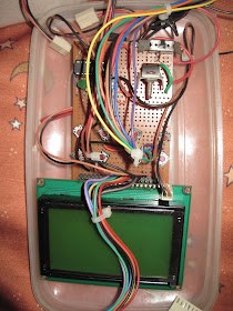
Here is the image of my hardware.
 |
| AVR Development Board |
 |
| USB Programmer |
Here is the top layout of my board.


